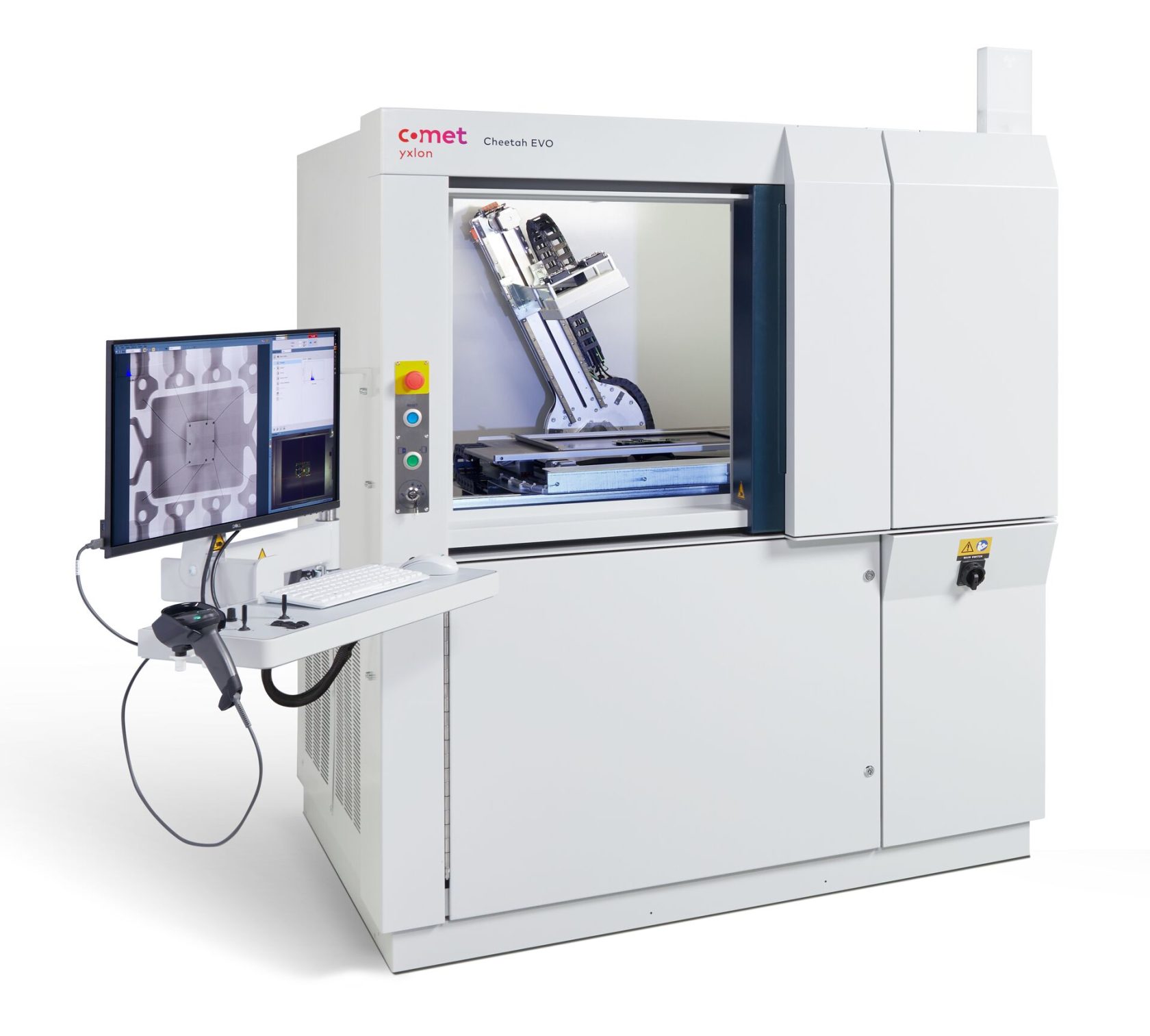
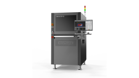
CA20
Compact and versatile solution from 2D and 3D microfocal inspection for semicon, advanced packaging and science and research.
- Designed for the semiconductor industry
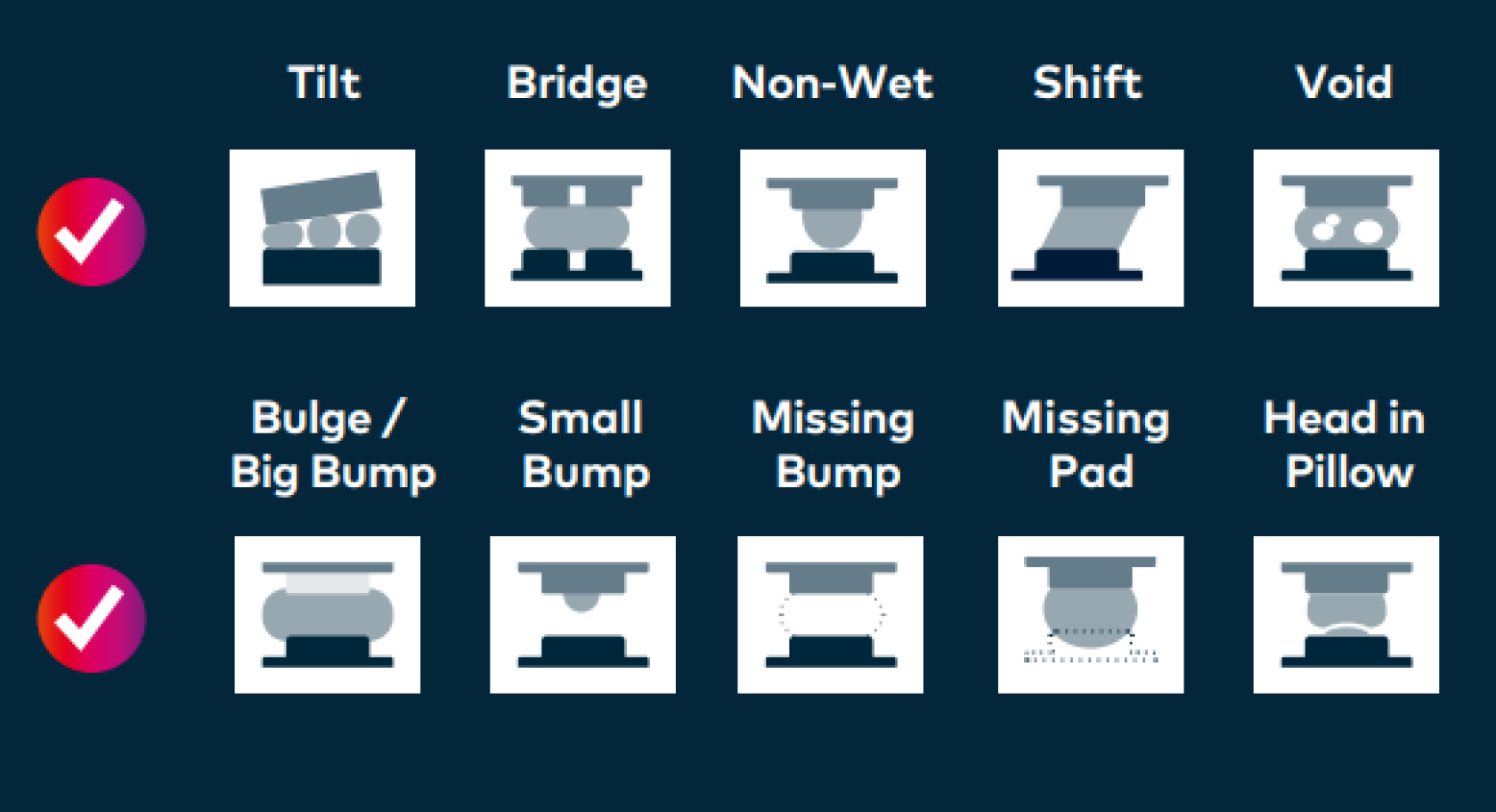
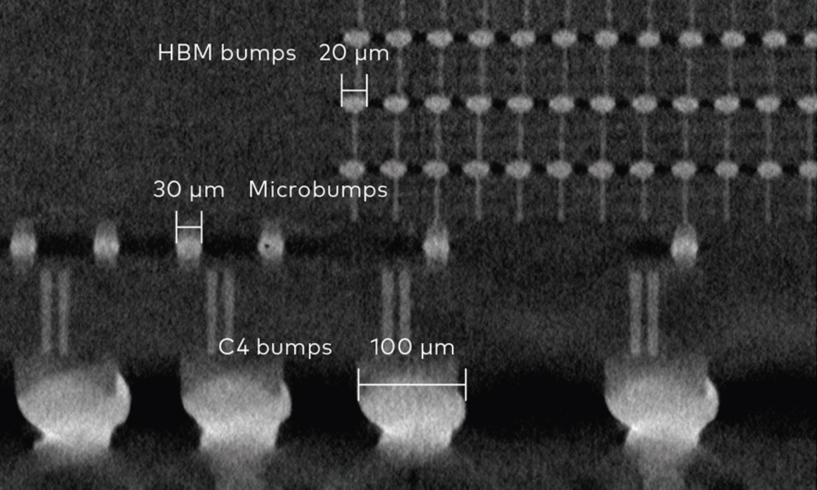
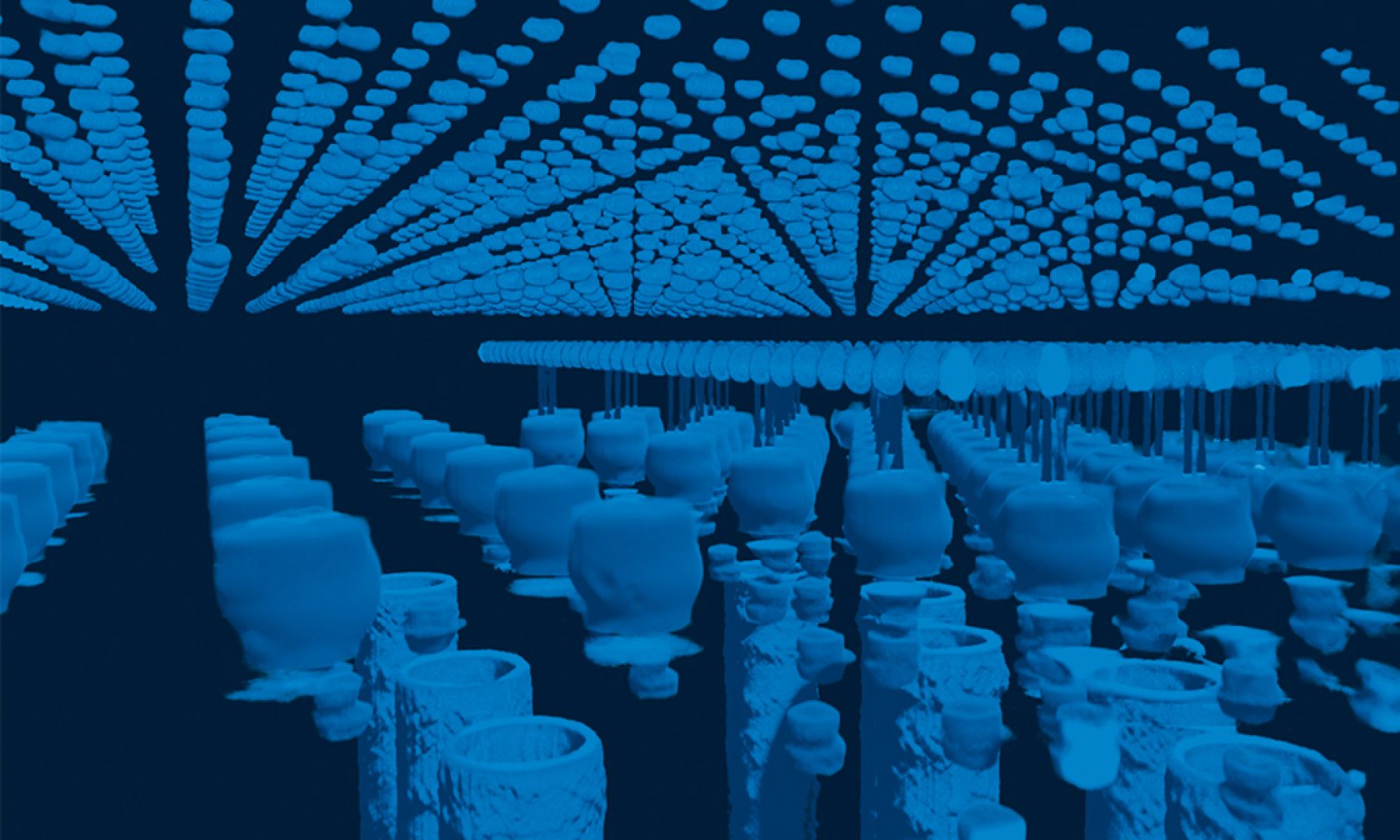
- Non-destructive technology for three-dimensional insights into solder bumps within minutes
- Repeatable results through reliable and accurate technology, designed to support a stable inspection routine
- Efficient software-assisted review including automated void analysis with Void Insights
- Dose Manager for the protection of X-ray sensitive components
- Sample size 435 mm (17´´)
- Resolution < 1 um
| Category | Semicon X-RAY inspection |
|---|---|
| Supplier | Comet YXLON |


Related categories
3D measurement for semicon applications
Koh Young offers a full range of inspection machines for semicon applications. Based on the standard platform the Meister S, Meister D and Meister...
Semiconductor testing products
FEINMETALL today has a leading position in the technology of probe cards for contacting semiconductors. The producst are also know as Probe...